 |
 |
 |
||||||||
|
Photoluminescence Imaging in Semiconductor Nanostructures Effects of nano-structure and localized states are investigated by spectroscopic imaging with subwavelength spatial resolution. Examples of materials of interest are quantum dots (a nano-engineered material targeted for solar cell applications in a number of schemes, such as impact ionization or multiple exciton generation, intermediate band solar cells, and improved thermoelectric materials). Major equipment consists of: an HR640 single grating spectrometer (high dispersion gratings), Princeton Instruments SPEC-10 back illuminated CCD, Millenia 5W pump laser and KML Ti:Sapphire femtosecond laser. A closed-loop piezo electric stage (PI 200mm x200mmx20mm range of motion) point-illuminates a Solid Immersion lens system housed in a liquid Helium bath-style cryostat (Oxford OptistatSXM) for spatially resolved photoluminescence imaging. This system will be extended to near-field imaging (as an example, see figure 3 below), wherein an optical fiber is tapered to a subwavelength dimension and used to illuminate and analyze semiconductor surfaces with subwavelength spatial resolution A closed cycle refrigeration unit and optical cryostat are also available for far-field PL measurements, and a time-correlated single photon counting card is on order for lifetime measurements. The system, and miscellaneous optics and associated instrumentation are housed on a 3rd 4x8 optical table. 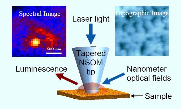
Related Publications [1] S. Smith, A. Mascarenhas, S. P. Ahrenkiel, M. C. Hanna, and J. M. Olson, "Spatially resolved below-gap emission in partially ordered GaxIn1-xP alloys," Phys. Rev. B 68 035310 (2003). [2] S. Smith, A. Mascarenhas, and J. M. Olson , "Magnetophotoluminescence of quantum confined states in ordered GaxIn1-xP with 200 nanometer resolution," Phys. Rev. B 68, 153202 (2003). [3] S. Smith, H.M. Cheong, B.D. Fluegel, J.F. Geisz, L.L. Kazmerski, A. Mascarenhas, "Spatially resolved photoluminescence in partially ordered GaInP2," Appl. Phys. Lett. 74 (5) 706-8 (1999).
| ||||||||||